Ceramic semiconductors power the equipment that manufactures modern electronics. Any shortage disrupts the global economy as consumer products depend on this technology. These materials withstand harsh processing environments where extreme temperatures, corrosive plasmas and demanding precision would destroy conventional metals or polymers. Silicon carbide (SiC) ceramics enable power transistors to operate at temperatures above 200°C and maintain stable performance up to 1700 degrees Celsius. Ceramic wafer handling systems, electrostatic chucks, ceramic packages for semiconductors and plasma generation tubes all rely on these materials. They provide the thermal stability and chemical resistance that modern manufacturing demands. This piece explores the types of ceramic materials used, their critical applications and why they remain indispensable for semiconductor production equipment.
What Are Ceramic Semiconductors in Manufacturing Equipment
Fine Ceramics, also referred to as advanced ceramics or engineered ceramics, represent inorganic, non-metallic materials formed through high-temperature processing that deliver exceptional performance in semiconductor manufacturing equipment. Traditional ceramics are associated with pottery. These materials possess superior thermal, mechanical and electrical characteristics engineered for industrial applications. These materials reach flatness levels below 1 μm and surface roughness of Ra ≥ 0.05 μm, making them suitable for extreme ultraviolet lithography and chemical vapor deposition processes.
Core Properties of Semiconductor Ceramics
Plasma corrosion resistance stands as the most critical attribute for ceramic components in semiconductor equipment. The semiconductor manufacturing process generates harsh plasma environments where this resistance prevents contamination from impurities that would create defective products. This property, combined with purity levels reaching 99.999% verified through glow discharge mass spectrometry, makes Fine Ceramics superior to glass, resins and metals for these applications.
Thermal performance distinguishes these materials in several ways. Alumina exhibits thermal conductivity ranging from 25 to 35 W/m·K depending on density and purity, while aluminum nitride delivers 70 to 170 W/m·K in high-purity forms without sintering aids. Silicon carbide achieves higher thermal conductivity between 100 and 200 W/m·K, exceeding alumina’s capabilities. These ceramics maintain dimensional stability and mechanical properties at temperatures where metals would soften or oxidize, with some formulations operating above 1,400 degrees Celsius.
Chemical stability in acidic and processing environments provides functionality for chamber liners and thermal insulation applications. Low thermal expansion coefficients ensure dimensional precision during temperature fluctuations inherent to deposition and etching processes.
How Ceramic Materials Differ from Metals and Polymers
Ceramics exhibit different mechanical behavior compared to metals and polymers. Silicon nitride demonstrates fracture toughness of around 5 to 8 MPa·m0.5. This is a big deal as it means that alumina’s 3 to 4 MPa·m0.5 enables components to withstand thermal cycling during rapid heating and quenching sequences. Metals deform under load while polymers absorb energy through flexibility.
Metals corrode over time and suffer from oxidation at elevated temperatures, whereas technical ceramics retain corrosion resistance without structural degradation. Polymers, despite being lightweight and economical, cannot withstand high-temperature semiconductor applications due to poor thermal and mechanical properties that lead to swelling, decomposition or loss of mechanical integrity when exposed to chemicals.
Electrical properties further differentiate these material classes. Technical ceramics provide insulation that withstands extreme voltages and temperatures, while metals conduct electricity, and certain ceramic compositions offer selective conductivity for specific applications. This versatility positions ceramic materials as irreplaceable in semiconductor manufacturing equipment where conventional materials fail.
Types of Ceramic Materials Used in Semiconductor Manufacturing
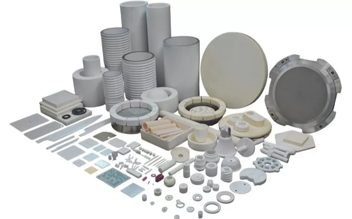
Different ceramic materials serve distinct functions in semiconductor manufacturing equipment. Each material gets selected for specific performance requirements. The selection depends on the combination of thermal, mechanical and chemical properties needed for each application.
Alumina (Al₂O₃) for Chamber Components
Alumina serves as the standard material in semiconductor fabrication facilities of all types and covers about 80% of applications. High-purity grades range from 99.99% to resist plasma to 99.7% for general-grade components. These ceramics operate at maximum temperatures that reach 1600°C with thermal conductivity between 30 and 33 W/m×K. Fabrication facilities deploy alumina in chamber parts, wafer transfer systems, and vacuum chucks. Mature supply chains and stable processing knowledge make this possible.
Silicon Carbide (SiC) Ceramic for High-Temperature Applications
Silicon carbide ceramic exhibits a hardness that only diamond and cubic boron nitride surpass. The material withstands decomposition temperatures that approach 2700°C. It maintains a low thermal expansion coefficient of 4 × 10⁻⁶K⁻¹ at the same time. SiC ceramic demonstrates superior plasma resistance compared to other ceramic carbides and generates minimal particles in fluorine-based plasma environments. Focus rings, susceptors, and chamber liners use this material despite costs five to ten times higher than alumina.
Aluminum Nitride (AlN) for Thermal Management
Aluminum nitride delivers thermal conductivity ranging from 170 to 230 W/mK. This exceeds alumina by a factor of five. Thin films deposited at low temperatures achieve cross-plane thermal conductivities that approach 90 Wm⁻¹K⁻¹. The material operates at maximum temperatures of 1200°C and provides electrical insulation properties. Electrostatic chucks, heater bodies, and ceramic packages for semiconductor use AlN to meet thermal dissipation requirements.
Silicon Nitride (Si₃N₄) for Structural Parts
Silicon nitride maintains reasonable fracture toughness up to 1400°C. Flexure strength reaches 900MPa. Material hardness measures 16GPa with Vickers hardness up to 1500 HV0.5. The ceramic wafer handling components and structural parts benefit from low thermal expansion and wear resistance.
Yttria and Advanced Ceramic Coatings
Yttrium oxide coatings demonstrate plasma consumption rates one-hundredth of quartz and one-tenth of alumina. The ceramic coatings market was valued at USD 680 million in 2024. Growth to USD 1,106 million by 2032 is projected. Materials require purity levels of 99.999% or higher to protect chamber components.
Critical Applications in Manufacturing Equipment
Manufacturing equipment deploys ceramic semiconductors across five critical application categories where material performance directly affects production yield and equipment longevity.
Ceramic Wafer Handling and Transfer Systems
Ceramic wafer transfer components function as end effectors on robotic arms that move wafers between processing stations. These ceramic components provide stiffness and high strength. Robot arms settle to final positions faster than aluminum alternatives and maintain precise positioning accuracy. The materials generate minimal particles in cleanroom environments, a requirement for contamination-sensitive fabrication processes. High-purity alumina and aluminum nitride compositions deliver the dimensional stability and thermal resistance needed for repeated handling cycles across temperature-varying chambers.
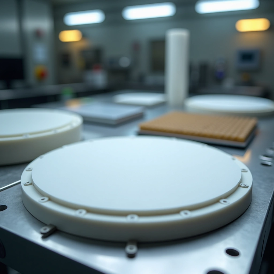
Electrostatic Chucks (ESCs) and Vacuum Components
Electrostatic chucks utilize embedded electrodes that generate attractive forces between the chuck structure and silicon wafers placed on the surface. These devices secure wafers during processing and provide flatness correction and active cooling. Alumina and aluminum nitride serve as main materials for ESC construction. The components withstand around 80,000 wafer passes before surface wear damages the electronic layers and requires refurbishment. Applications include photolithography, chemical vapor deposition, plasma etching, and atomic layer deposition processes.
Process Chamber Liners and Interior Surfaces
Chamber liners protect metal walls from plasma exposure and maintain thermal management while preventing contamination. CVD silicon carbide materials achieve purity levels of 99.999% as verified by glow discharge mass spectrometry. The non-porous microstructure provides superior resistance to plasma etching and minimal particle shedding throughout the component’s service life. High-purity alumina chambers deliver excellent plasma corrosion resistance with reliable plasma impedance characteristics. Edge rings, isolator rings, and shield rings employ these ceramics across deposition and etch systems.
Ceramic Packages for Semiconductors and Heat Dissipation
Ceramic packages for semiconductors use high thermal conductivity and coefficients of thermal expansion that match semiconductor chip materials. The materials provide superior strength, stability, and rigidity compared to alternative packaging solutions. High strength permits thinner cavity walls and device miniaturization. Assembly options include wire bonding and flip-chip bonding at the chip level. Board-level configurations include LCC, QFP, PGA, DIP, and BGA formats. Applications range from mass-produced devices to precision equipment requiring maximum reliability.
Plasma Generation and Introduction Tubes
Plasma discharge tubes contain and direct plasma during generation processes. Aluminum nitride produces the lowest tube temperatures and mechanical stresses among four evaluated ceramic materials. Monolithic aluminum nitride structures demonstrate operational capability at power levels reaching 250 kW. The material’s thermal conductivity of 92 W/(m·K) at room temperature, combined with a melting point of 1900°C in vacuum, makes sustained high-repetition-rate plasma discharge operation possible. Alumina also serves in plasma generation applications due to its dielectric properties and resistance to high temperatures exceeding 1000°C.
Why Ceramic Semiconductors Are Essential for Modern Equipment
Semiconductor fabrication processes expose equipment to conditions that degrade conventional materials faster. This necessitates ceramic solutions in major manufacturing operations.
Plasma Resistance in Harsh Processing Environments
Plasma corrosion resistance prevents contamination from unintended impurities that cause defective products. High-density plasma environments accelerate erosion of chambers, liners, rings, shutters, and windows during etching and deposition processes. Yttria-based coatings produced through suspension vacuum plasma spraying demonstrate approximately four times greater plasma etching resistance compared to conventional atmospheric plasma spray methods. Porosity stays below 1%, and hardness reaches 605 HV.
Thermal Stability at Temperatures Above 1000°C
Ceramics withstand temperatures ranging from 1200°C to 1800°C and maintain structural integrity. Alumina operates at thermal resistance levels of 1500°C or more. Silicon carbide maintains strength at extreme temperatures where metals would fail.
Dimensional Precision and Low Particle Generation
Ceramics remain dust-free compared to organic materials and generate minimal particles during processing cycles. Dense microstructures with controlled particle size distributions ensure consistent dimensional stability.
Chemical Resistance to Corrosive Gasses
Silicon carbide and alumina exhibit very low chemical solubility in acids and bases. Materials resist fluorine-based plasmas, chlorine ions, and oxygen radicals that attack quartz and lower-grade ceramics.
Extended Equipment Lifetime and Reliability
Ceramic components last substantially longer than metal or polymer parts due to resistance against wear, corrosion, and plasma exposure. This durability reduces unscheduled maintenance and minimizes contamination risks.
Conclusion
Ceramic semiconductors remain irreplaceable in modern manufacturing equipment. Their plasma resistance, thermal stability up to 1800°C, and chemical durability enable production that metals and polymers cannot achieve reliably. Alumina, silicon carbide, aluminum nitride, and silicon nitride each deliver specialized performance in wafer handling systems, electrostatic chucks, chamber components, and plasma generation tubes. These materials are the foundations of semiconductor fabrication and ensure production efficiency with equipment longevity that conventional materials cannot match.
FAQs
Q1. What makes ceramic materials important for semiconductor manufacturing equipment? Ceramic materials provide exceptional plasma resistance, thermal stability up to 1800°C, and chemical durability that metals and polymers cannot match. They withstand harsh processing environments involving extreme temperatures, corrosive plasmas, and demanding precision requirements, making them essential for reliable semiconductor production.
Q2. Which ceramic materials are commonly used in semiconductor equipment and why? Alumina (Al₂O₃) is the most widely used, covering about 80% of applications due to its reliability and cost-effectiveness. Silicon carbide (SiC) offers superior high-temperature performance and plasma resistance. Aluminum nitride (AlN) provides excellent thermal conductivity for heat management, while silicon nitride (Si₃N₄) delivers exceptional strength for structural components.
Q3. How do ceramics contribute to energy efficiency in semiconductor manufacturing? Ceramics optimize energy use through their high thermal conductivity and low thermal expansion properties. Materials like aluminum nitride efficiently dissipate heat, reducing power consumption during processing. Their dimensional stability at extreme temperatures also minimizes energy waste from thermal cycling and equipment recalibration.
Q4. What are the main applications of ceramic semiconductors in manufacturing equipment? Ceramic semiconductors are used in wafer handling and transfer systems, electrostatic chucks for securing wafers during processing, process chamber liners that protect equipment from plasma exposure, ceramic packages for heat dissipation, and plasma generation tubes that contain and direct plasma during fabrication processes.
Q5. How do ceramic components extend equipment lifetime in semiconductor manufacturing? Ceramic components last significantly longer than metal or polymer alternatives due to their superior resistance against wear, corrosion, and plasma exposure. This durability reduces unscheduled maintenance, minimizes contamination risks, and ensures consistent performance throughout extended production cycles, ultimately improving manufacturing efficiency and reliability.